- 您现在的位置:买卖IC网 > Sheet目录3890 > PIC16C717T-E/SS (Microchip Technology)IC MCU OTP 2KX14 A/D PWM 20SSOP
2002 Microchip Technology Inc.
DS41120B-page 109
PIC16C717/770/771
After the A/D module has been configured as desired
and the analog input channels have their correspond-
ing TRIS bits selected for port inputs, the selected
channel must be acquired before conversion is
started. The A/D conversion cycle can be initiated by
setting the GO/DONE bit. The A/D conversion begins
and lasts for 13TAD. The following steps should be fol-
lowed for performing an A/D conversion:
1.
Configure port pins:
Configure Analog Input mode (ANSEL)
Configure pin as input (TRISA or TRISB)
2.
Configure the A/D module
Configure A/D Result Format / voltage refer-
ence (ADCON1)
Select A/D input channel (ADCON0)
Select A/D conversion clock (ADCON0)
Turn on A/D module (ADCON0)
3.
Configure A/D interrupt (if required)
Clear ADIF bit
Set ADIE bit
Set PEIE bit
Set GIE bit
4.
Wait the required acquisition time.
5.
START conversion
Set GO/DONE bit (ADCON0)
6.
Wait 13TAD until A/D conversion is complete, by
either:
Polling for the GO/DONE bit to be cleared
OR
Waiting for the A/D interrupt
7.
Read A/D Result registers (ADRESH and
ADRESL), clear ADIF if required.
8.
For next conversion, go to step 1, step 2 or step
3 as required.
Clearing the GO/DONE bit during a conversion will
abort the current conversion. The ADRESH and
ADRESL registers will be updated with the partially
completed
A/D
conversion
value.
That
is,
the
ADRESH and ADRESL registers will contain the value
of the current incomplete conversion.
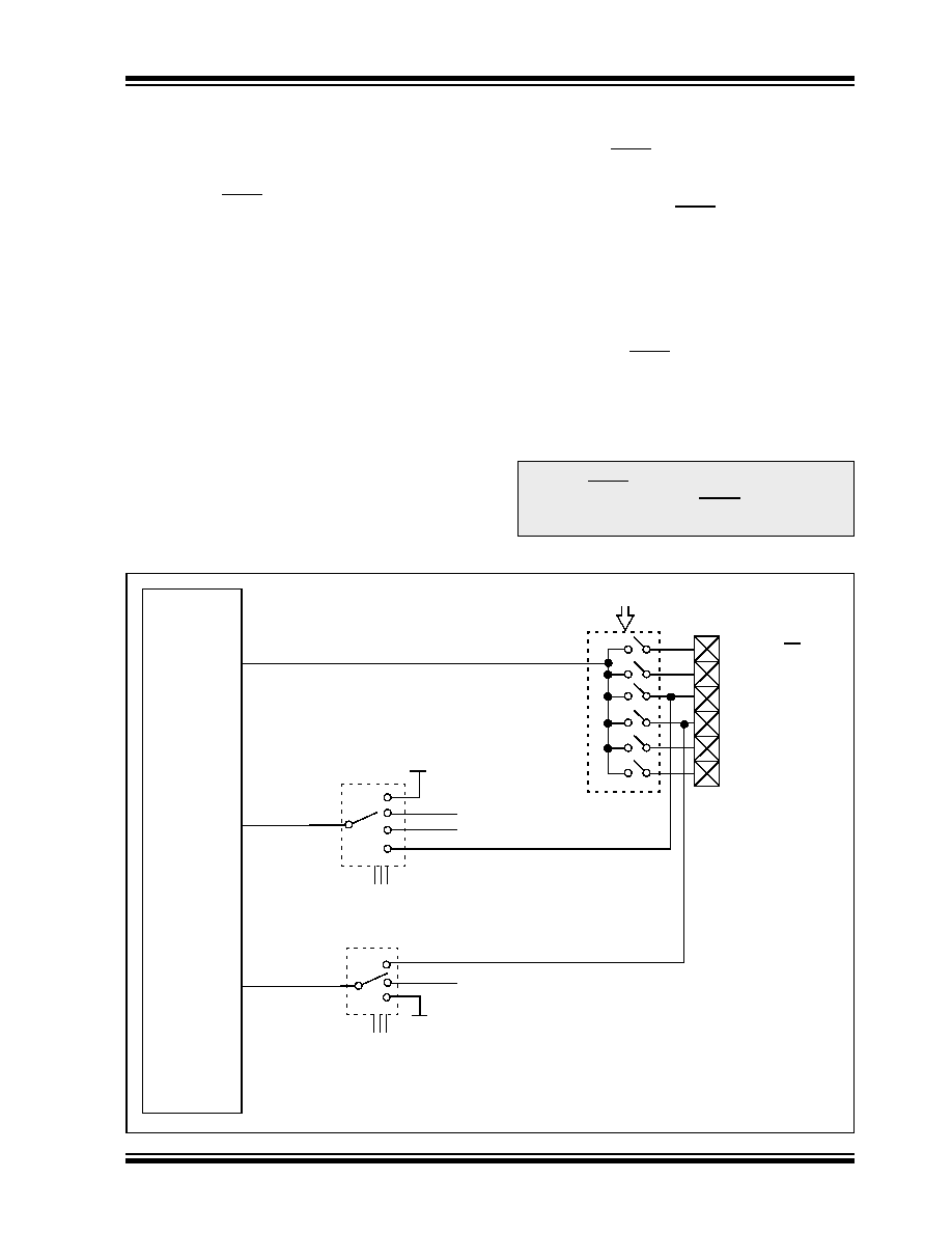
FIGURE 11-3:
A/D BLOCK DIAGRAM
Note:
Do not set the ADON bit and the GO/
DONE bit in the same instruction. Doing so
will cause the GO/DONE bit to be automat-
ically cleared.
(INPUT VOLTAGE)
VAIN
VREF+
(REFERENCE
VOLTAGE
+)
AVDD
VCFG<2:0>
CHS<3:0>
RB1/AN5/SS
RB0/AN4/INT
RA3/AN3/VREF+/VRH
RA2/AN2/VREF-/VRL
RA1/AN1
RA0/AN0
A/D
CONVERTER
VREF-
(REFERENCE
VOLTAGE
-)
AVSS
VCFG<2:0>
VRH
VRL
发布紧急采购,3分钟左右您将得到回复。
相关PDF资料
PIC16LC770T-E/SO
IC MCU OTP 2KX14 A/D PWM 20SOIC
PIC16C771T/SO
IC MCU OTP 4KX14 A/D PWM 20SOIC
PIC16LC717T-I/SS
IC MCU OTP 2KX14 A/D PWM 20SSOP
PIC16C717T/SS
IC MCU OTP 2KX14 A/D PWM 20SSOP
PIC16LC770T-I/SO
IC MCU OTP 2KX14 A/D PWM 20SOIC
PIC16LC771T-E/SS
IC MCU OTP 4KX14 A/D PWM 20SSOP
PIC16C771T-E/SS
IC MCU OTP 4KX14 A/D PWM 20SSOP
PIC16LC771T-I/SO
IC MCU OTP 4KX14 A/D PWM 20SOIC
相关代理商/技术参数
PIC16C717T-I/SO
功能描述:8位微控制器 -MCU 3.5KB 256 RAM 16 I/O RoHS:否 制造商:Silicon Labs 核心:8051 处理器系列:C8051F39x 数据总线宽度:8 bit 最大时钟频率:50 MHz 程序存储器大小:16 KB 数据 RAM 大小:1 KB 片上 ADC:Yes 工作电源电压:1.8 V to 3.6 V 工作温度范围:- 40 C to + 105 C 封装 / 箱体:QFN-20 安装风格:SMD/SMT
PIC16C717T-I/SS
功能描述:8位微控制器 -MCU 3.5KB 256 RAM 16 I/O RoHS:否 制造商:Silicon Labs 核心:8051 处理器系列:C8051F39x 数据总线宽度:8 bit 最大时钟频率:50 MHz 程序存储器大小:16 KB 数据 RAM 大小:1 KB 片上 ADC:Yes 工作电源电压:1.8 V to 3.6 V 工作温度范围:- 40 C to + 105 C 封装 / 箱体:QFN-20 安装风格:SMD/SMT
PIC16C71T-04/SO
功能描述:8位微控制器 -MCU 1.75KB 36 RAM 13 I/O 4MHz SOIC18 RoHS:否 制造商:Silicon Labs 核心:8051 处理器系列:C8051F39x 数据总线宽度:8 bit 最大时钟频率:50 MHz 程序存储器大小:16 KB 数据 RAM 大小:1 KB 片上 ADC:Yes 工作电源电压:1.8 V to 3.6 V 工作温度范围:- 40 C to + 105 C 封装 / 箱体:QFN-20 安装风格:SMD/SMT
PIC16C71T-04I/SO
功能描述:8位微控制器 -MCU 1.75KB 36 RAM 13 I/O 4MHz Ind Temp SOIC18 RoHS:否 制造商:Silicon Labs 核心:8051 处理器系列:C8051F39x 数据总线宽度:8 bit 最大时钟频率:50 MHz 程序存储器大小:16 KB 数据 RAM 大小:1 KB 片上 ADC:Yes 工作电源电压:1.8 V to 3.6 V 工作温度范围:- 40 C to + 105 C 封装 / 箱体:QFN-20 安装风格:SMD/SMT
PIC16C71T-20/SO
功能描述:8位微控制器 -MCU 1.75KB 36 RAM 13 I/O RoHS:否 制造商:Silicon Labs 核心:8051 处理器系列:C8051F39x 数据总线宽度:8 bit 最大时钟频率:50 MHz 程序存储器大小:16 KB 数据 RAM 大小:1 KB 片上 ADC:Yes 工作电源电压:1.8 V to 3.6 V 工作温度范围:- 40 C to + 105 C 封装 / 箱体:QFN-20 安装风格:SMD/SMT
PIC16C71T-20I/SO
功能描述:8位微控制器 -MCU 1.75KB 36 RAM 13 I/O RoHS:否 制造商:Silicon Labs 核心:8051 处理器系列:C8051F39x 数据总线宽度:8 bit 最大时钟频率:50 MHz 程序存储器大小:16 KB 数据 RAM 大小:1 KB 片上 ADC:Yes 工作电源电压:1.8 V to 3.6 V 工作温度范围:- 40 C to + 105 C 封装 / 箱体:QFN-20 安装风格:SMD/SMT
PIC16C72/JW
功能描述:8位微控制器 -MCU 3.5KB 128 RAM 22 I/O RoHS:否 制造商:Silicon Labs 核心:8051 处理器系列:C8051F39x 数据总线宽度:8 bit 最大时钟频率:50 MHz 程序存储器大小:16 KB 数据 RAM 大小:1 KB 片上 ADC:Yes 工作电源电压:1.8 V to 3.6 V 工作温度范围:- 40 C to + 105 C 封装 / 箱体:QFN-20 安装风格:SMD/SMT
PIC16C72-04/SO
功能描述:8位微控制器 -MCU 3.5KB 128 RAM 22 I/O RoHS:否 制造商:Silicon Labs 核心:8051 处理器系列:C8051F39x 数据总线宽度:8 bit 最大时钟频率:50 MHz 程序存储器大小:16 KB 数据 RAM 大小:1 KB 片上 ADC:Yes 工作电源电压:1.8 V to 3.6 V 工作温度范围:- 40 C to + 105 C 封装 / 箱体:QFN-20 安装风格:SMD/SMT